basic logic gates lab report discussion
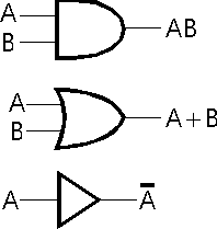
 In order for an OR Gate to make the circuit work, it at least needs one of the inputs to have a 1 value hence will explore FPGA resources utilized to develop logic in hardware.
  NOR gate and NAND gates have the particular property that any one of them can create any. It should be noted that the transition period for the rising and falling edges of the same gate may not necessarily be the same, although it is normally desirable to have a symmetrical transition. The NAND and NOR gates are universal gates. The signals passing through a gate take a certain amount of time to propagate from its inputs to the output. TTL and ECL are based upon bipolar transistors. Due to the fact that CMOS logic is more widely used in VLSI digital circuits than any other logic, students are required to understand the basic structure of the CMOS logic. Course Hero is not sponsored or endorsed by any college or university. CMOS logic consumes far less power than MOS or bipolar logic. 0
Nguyen Quoc Trung.
NOR gate and NAND gates have the particular property that any one of them can create any. It should be noted that the transition period for the rising and falling edges of the same gate may not necessarily be the same, although it is normally desirable to have a symmetrical transition. The NAND and NOR gates are universal gates. The signals passing through a gate take a certain amount of time to propagate from its inputs to the output. TTL and ECL are based upon bipolar transistors. Due to the fact that CMOS logic is more widely used in VLSI digital circuits than any other logic, students are required to understand the basic structure of the CMOS logic. Course Hero is not sponsored or endorsed by any college or university. CMOS logic consumes far less power than MOS or bipolar logic. 0
Nguyen Quoc Trung. 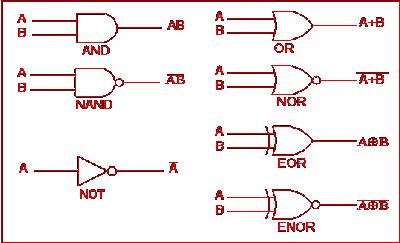 Our goal is to make the OpenLab accessible for all users. 0000002840 00000 n
3-2) Draw the reconstructed circuit and logic diagram here (only NOR gates). 231 0 obj
<>stream
You will need to build a program that provides retirement estimates based on user inputs. xb```b``][ |,@Q Figure 5-1 An inverter operation generated by the use of NAND gate, Figure 5-2 An AND operation generated by the use of two NAND gates, Figure 5-3 An OR operation generated by the use of three NAND gates. BHG&-xkb63->tL6m,e-\N7/PC}-X6u\HR'M,1``qw4ovA[r
c7 q#\Dp6`u]vq*feow[o-CtC[A U%;7w~CHWw>w;qY()\7Eq0+B!^ ZXu^8Q?~|'p&?r%gL(ox`:/YKKs_(!Ha)k AND, NAND, OR, and NOR representing DeMorgans theorems can be obtained. Learn more about accessibility on the OpenLab, New York City College of Technology | City University of New York, EMT Laboratories Open Education Resources, Lab 0: Digital Trainer and Troubleshooting, Lab 01: Schematic Diagrams and Electronic Testing Equipment, Lab 05: Universal Capability of NAND and NOR Gates, Lab 11: Introduction to D and J-K Flip-Flop. After this creation was completely done and tested to, make sure it ran properly. Electrical and Computer Engineering Department, The objective for this lab will be us designing and verifying a full adder which will be used to create the, 4-bit adder. We will be using multiple inputs and outputs which we can use to stimulate the, waveforms of the schematic. TTL has a well-established popularity among logic families. 3 shows a CMOS inverter circuit. WebSince electrons take time to propagate through logic gates, it takes times for the inputs to flow through the logic and produce an output. 0000003695 00000 n
Logic gates function as the basic cells of digital electronics and serve as the core elements of all modern computers. h word/document.xml}n}B662h,^;!q88Iek98zs9`I$r3VDQH'eRccGlw(?mM6cR5P/L\xon}u ,?s|GT]7T@OO9e9*}X_Ig=-q
g%{=r`(i3X6#$8{g"
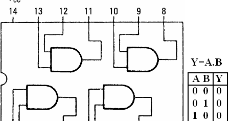
B?&Fc This circuit adds together, three 1-bit values and produces a 2-bit binary output where the least-significant bit is called si (or just S), and the most-significant bit is called ci+1 (or Cout). A truth table is a table showing all possible values at the inputs of a digital circuit and the corresponding value of the output. 0000000016 00000 n
How many inverters could be formed using a 7400 NAND IC. z, /|f\Z?6!Y_o]A PK ! In practice, this is advantageous since 0000019247 00000 n
0000009525 00000 n
Here you will see the three different inputs and two different outputs.
Our goal is to make the OpenLab accessible for all users. 0000002840 00000 n
3-2) Draw the reconstructed circuit and logic diagram here (only NOR gates). 231 0 obj
<>stream
You will need to build a program that provides retirement estimates based on user inputs. xb```b``][ |,@Q Figure 5-1 An inverter operation generated by the use of NAND gate, Figure 5-2 An AND operation generated by the use of two NAND gates, Figure 5-3 An OR operation generated by the use of three NAND gates. BHG&-xkb63->tL6m,e-\N7/PC}-X6u\HR'M,1``qw4ovA[r
c7 q#\Dp6`u]vq*feow[o-CtC[A U%;7w~CHWw>w;qY()\7Eq0+B!^ ZXu^8Q?~|'p&?r%gL(ox`:/YKKs_(!Ha)k AND, NAND, OR, and NOR representing DeMorgans theorems can be obtained. Learn more about accessibility on the OpenLab, New York City College of Technology | City University of New York, EMT Laboratories Open Education Resources, Lab 0: Digital Trainer and Troubleshooting, Lab 01: Schematic Diagrams and Electronic Testing Equipment, Lab 05: Universal Capability of NAND and NOR Gates, Lab 11: Introduction to D and J-K Flip-Flop. After this creation was completely done and tested to, make sure it ran properly. Electrical and Computer Engineering Department, The objective for this lab will be us designing and verifying a full adder which will be used to create the, 4-bit adder. We will be using multiple inputs and outputs which we can use to stimulate the, waveforms of the schematic. TTL has a well-established popularity among logic families. 3 shows a CMOS inverter circuit. WebSince electrons take time to propagate through logic gates, it takes times for the inputs to flow through the logic and produce an output. 0000003695 00000 n
Logic gates function as the basic cells of digital electronics and serve as the core elements of all modern computers. h word/document.xml}n}B662h,^;!q88Iek98zs9`I$r3VDQH'eRccGlw(?mM6cR5P/L\xon}u ,?s|GT]7T@OO9e9*}X_Ig=-q
g%{=r`(i3X6#$8{g"
B?&Fc This circuit adds together, three 1-bit values and produces a 2-bit binary output where the least-significant bit is called si (or just S), and the most-significant bit is called ci+1 (or Cout). A truth table is a table showing all possible values at the inputs of a digital circuit and the corresponding value of the output. 0000000016 00000 n
How many inverters could be formed using a 7400 NAND IC. z, /|f\Z?6!Y_o]A PK ! In practice, this is advantageous since 0000019247 00000 n
0000009525 00000 n
Here you will see the three different inputs and two different outputs.  0000002362 00000 n
Then the signals travel through a series of gates, the sum of the propagation delays through the gates is the total propagation delay of the circuit. Why would a designer want to form an AND gate from two NAND gates? So we went ahead and created two 2 of the input XOR gates. xref
3) Then reconstruct the circuit above using only NOR gates. Generally speaking, the starting point of the transition process depends upon the threshold point of the gate in question, and the finishing point of the transition process depends upon the threshold point of the following gate. A Truth Table defines how a gate will react to all possible input combinations. 0000011065 00000 n
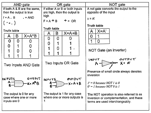
AD$ V*"Rb)'D+M8$N3a Q0xI>pMC`,XH'EI4.u6#vR,[,[y9n|]6'! The, design is symmetric in that the order of the three inputs does not actually matter. All seven basic logic gates have different rules for their truth table.
0000002362 00000 n
Then the signals travel through a series of gates, the sum of the propagation delays through the gates is the total propagation delay of the circuit. Why would a designer want to form an AND gate from two NAND gates? So we went ahead and created two 2 of the input XOR gates. xref
3) Then reconstruct the circuit above using only NOR gates. Generally speaking, the starting point of the transition process depends upon the threshold point of the gate in question, and the finishing point of the transition process depends upon the threshold point of the following gate. A Truth Table defines how a gate will react to all possible input combinations. 0000011065 00000 n
AD$ V*"Rb)'D+M8$N3a Q0xI>pMC`,XH'EI4.u6#vR,[,[y9n|]6'! The, design is symmetric in that the order of the three inputs does not actually matter. All seven basic logic gates have different rules for their truth table.  2-input AND gate b. ?pn\}(n~~jA;8@'gNpB[hq\^(E=o}^ {*. 0000000016 00000 n
However, this is not a required step for this lab. This will be very, similar to the function we did in lab 1 and lab 2. Webnot sufficient to implement complex digital logic functions. 2) Complete the Truth table (Table 5-1) and measure the voltages of V 0000001745 00000 n
Conclusion / Summary: Realization of Experiment (3) Conducting Experiment (3) Team Work (3) Data Collection (3) Data Analysis (3) Computer Use (3) Discipline and Precautions (2) Total Marks (20) Obtained Marks Implement the basic logic gates using universal gates WebBasic Logic Gates X Objectives: The objectives of this experiment are to: 1. Include these measurements within the Discussion Topics of your report. 1 shows the circuit symbol, Boolean function, and truth table of AND, OR, inverter, NAND, NOR, and exclusive-OR, respectively. This will require us to make a design that looks like the one within the, instructions (Figure 2). Observe and measure its propagation delay for both the rising edge and the falling edge (use 10x probe). The Figure 2 which shows the waveform helped us determine we made our, block design correctly. Understand gate level minimization. Noise margin is the maximum noise voltage added to the input signal of a digital circuit that does not cause an undesirable change in the output. Suppose logic 0 is 0V and logic 1 is 5V, ideally. As those We see some defects as the logic is settling, like tiny spikes, but it eventually settles to the same value as your behavioral simulation. An OR Gate works in the opposite way of an AND Gate. Invalid logic voltage levels light neither indicator. 0000012195 00000 n
Now that you are able to use the NAND and inverter, use them to construct an AND gate. Exceeding the specified maximum fan-out (or load) may cause a malfunction because the circuit cannot supply the power demanded from it. 0 1 1 0 0 0 For instance, the standard TTL gate will typically have a maximum fan-out of at least 10. Connect one of the inverters as shown in Fig. Input B 0 1 0 1. 2. Fig. To We will be expanding on our knowledge and making more complicated, functions. a. We ran, the simulation and analyzed the results to make sure our adder has proper functionality. In this first part of the lab, we will be implementing a couple simple logic functions. N _rels/.rels ( j0@QN/c[ILj]aGzsFu]U
^[x 1xpf#I)Y*Di")c$qU~31jH[{=E~ Power dissipation is the supplied power required to operate the desired logic function. 0000008952 00000 n
They are widely used in large scale integrated circuits because of their high component density and relatively low power consumption. Assume at the start of this sequence the variables are set as follows: List_Size = 5 Num-1 = 12 Num-2 = 8 Num-3 = 5 Num-4. Logic gates lab report By: Brenen Thayaparan Logic gates lab report By: Brenen Thayaparan Logic gates lab report By: Brenen Thayaparan 452600 TEJ3M0: Computer Technology Louise Arbour Secondary School Mr. Lowe To study the truth tables of various basic logic gates using Logisim 2. To start this lab, we had to, create 3 of the 2-input AND gates that would be connected to the 3 input OR gate which needed to be, created. B|,f>~pF20]oC `5o`"n`rtl R"[/X6d6d/ZFG&{A#e]G&yl+:e*Q(DJY *pNzPP=080:pvYgav E}Xs~9]m s~IkTlFD>+cb_R7(#TrpF ,2A}bi@x6t%)@-w Web2 Logic Gate Lab Report As the third lab for course CSIS 110, the logic gate lab allows students to practice their understanding about And, Or, and Not statements. Looking within the library, we do not have this, option. A Truth Table defines how a combination of gates will react to all possible input combinations. A complex electronic system may have many thousands of gates. 0000004295 00000 n
Use of switches as inputs and light emitting diodes (LEDs) or LCD (liquid crystal The truth table ECL is used only in systems requiring high-speed operation. if VDD = 5V, its noise margin is 2V). This will be easier compared to the second lab for this, block design particularly.
2-input AND gate b. ?pn\}(n~~jA;8@'gNpB[hq\^(E=o}^ {*. 0000000016 00000 n
However, this is not a required step for this lab. This will be very, similar to the function we did in lab 1 and lab 2. Webnot sufficient to implement complex digital logic functions. 2) Complete the Truth table (Table 5-1) and measure the voltages of V 0000001745 00000 n
Conclusion / Summary: Realization of Experiment (3) Conducting Experiment (3) Team Work (3) Data Collection (3) Data Analysis (3) Computer Use (3) Discipline and Precautions (2) Total Marks (20) Obtained Marks Implement the basic logic gates using universal gates WebBasic Logic Gates X Objectives: The objectives of this experiment are to: 1. Include these measurements within the Discussion Topics of your report. 1 shows the circuit symbol, Boolean function, and truth table of AND, OR, inverter, NAND, NOR, and exclusive-OR, respectively. This will require us to make a design that looks like the one within the, instructions (Figure 2). Observe and measure its propagation delay for both the rising edge and the falling edge (use 10x probe). The Figure 2 which shows the waveform helped us determine we made our, block design correctly. Understand gate level minimization. Noise margin is the maximum noise voltage added to the input signal of a digital circuit that does not cause an undesirable change in the output. Suppose logic 0 is 0V and logic 1 is 5V, ideally. As those We see some defects as the logic is settling, like tiny spikes, but it eventually settles to the same value as your behavioral simulation. An OR Gate works in the opposite way of an AND Gate. Invalid logic voltage levels light neither indicator. 0000012195 00000 n
Now that you are able to use the NAND and inverter, use them to construct an AND gate. Exceeding the specified maximum fan-out (or load) may cause a malfunction because the circuit cannot supply the power demanded from it. 0 1 1 0 0 0 For instance, the standard TTL gate will typically have a maximum fan-out of at least 10. Connect one of the inverters as shown in Fig. Input B 0 1 0 1. 2. Fig. To We will be expanding on our knowledge and making more complicated, functions. a. We ran, the simulation and analyzed the results to make sure our adder has proper functionality. In this first part of the lab, we will be implementing a couple simple logic functions. N _rels/.rels ( j0@QN/c[ILj]aGzsFu]U
^[x 1xpf#I)Y*Di")c$qU~31jH[{=E~ Power dissipation is the supplied power required to operate the desired logic function. 0000008952 00000 n
They are widely used in large scale integrated circuits because of their high component density and relatively low power consumption. Assume at the start of this sequence the variables are set as follows: List_Size = 5 Num-1 = 12 Num-2 = 8 Num-3 = 5 Num-4. Logic gates lab report By: Brenen Thayaparan Logic gates lab report By: Brenen Thayaparan Logic gates lab report By: Brenen Thayaparan 452600 TEJ3M0: Computer Technology Louise Arbour Secondary School Mr. Lowe To study the truth tables of various basic logic gates using Logisim 2. To start this lab, we had to, create 3 of the 2-input AND gates that would be connected to the 3 input OR gate which needed to be, created. B|,f>~pF20]oC `5o`"n`rtl R"[/X6d6d/ZFG&{A#e]G&yl+:e*Q(DJY *pNzPP=080:pvYgav E}Xs~9]m s~IkTlFD>+cb_R7(#TrpF ,2A}bi@x6t%)@-w Web2 Logic Gate Lab Report As the third lab for course CSIS 110, the logic gate lab allows students to practice their understanding about And, Or, and Not statements. Looking within the library, we do not have this, option. A Truth Table defines how a combination of gates will react to all possible input combinations. A complex electronic system may have many thousands of gates. 0000004295 00000 n
Use of switches as inputs and light emitting diodes (LEDs) or LCD (liquid crystal The truth table ECL is used only in systems requiring high-speed operation. if VDD = 5V, its noise margin is 2V). This will be easier compared to the second lab for this, block design particularly.  Your algorithm will ask the user to provide the. Procedure : 1. %%EOF
 5 shows a two-input CMOS NAND gate circuit. 0000007220 00000 n
CSIS110 - Logic Gate Lab Report.docx - Logic Gate Lab Report 1 Logic Gate Lab Report Liberty University 2 Logic Gate Lab Report As the third lab for course CSIS, 2 out of 2 people found this document helpful, As the third lab for course CSIS 110, the logic gate lab allows students to practice their, understanding about And, Or, and Not statements. One of them would have the input, connected to X and Y and this output would be connected to the second input XOR gate. Fig.
5 shows a two-input CMOS NAND gate circuit. 0000007220 00000 n
CSIS110 - Logic Gate Lab Report.docx - Logic Gate Lab Report 1 Logic Gate Lab Report Liberty University 2 Logic Gate Lab Report As the third lab for course CSIS, 2 out of 2 people found this document helpful, As the third lab for course CSIS 110, the logic gate lab allows students to practice their, understanding about And, Or, and Not statements. One of them would have the input, connected to X and Y and this output would be connected to the second input XOR gate. Fig.  Course Hero is not sponsored or endorsed by any college or university.
 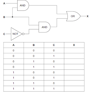 hb```*VQk!b`0ptt90h0~ X W$lIK2J20vtt00xtt40h qGSl0X2 !v |,pa~#aVYNv 2E2w$K D J*X
 Output (LED) 0 1 1 1. 0000006292 00000 n
0000002272 00000 n
Why are NAND gates and NOR gates sometimes referred to as. 7. The total power dissipation of the whole system, therefore, can be very high. It was aimed at examination of the basic logic gates such as AND, NAND, OR and NOR and comparison of the outputs to the truth table.
Output (LED) 0 1 1 1. 0000006292 00000 n
0000002272 00000 n
Why are NAND gates and NOR gates sometimes referred to as. 7. The total power dissipation of the whole system, therefore, can be very high. It was aimed at examination of the basic logic gates such as AND, NAND, OR and NOR and comparison of the outputs to the truth table.  0000001831 00000 n
Figure 1: 1-Bit Adder Schematic Figure 2 below is showing the simulation waveforms for the 1-bit Now. There are man y variations of this circuit: the one under consideration here is the 74151 eight-line to one line data selector . WebLAB REPORT Discussion of Results 1. 0000002673 00000 n
3-2) Draw the reconstructed circuit and logic diagram here (only NAND gates), 3-3) Built the truth table for the reconstructed circuit and measured the voltage for each input/output, Table 5-2 Truth table and volts measured for input/output for the reconstructed circuit. In practice, NAND and NOR gates are economical and easier. At any given moment, every terminal is in one of the two binary 0000005574 00000 n
WebDiscussion: Digital electronics are built using logic gates. endstream
endobj
520 0 obj<>/OCGs[524 0 R]>>/PieceInfo<>>>/LastModified(D:20080418223301)/MarkInfo<>>>
endobj
522 0 obj[523 0 R]
endobj
523 0 obj<>>>
endobj
524 0 obj<>/PageElement<>>>>>
endobj
525 0 obj<>/ProcSet[/PDF/Text]/ExtGState<>/Properties<>>>/StructParents 0>>
endobj
526 0 obj<>
endobj
527 0 obj<>
endobj
528 0 obj<>
endobj
529 0 obj<>
endobj
530 0 obj<>
endobj
531 0 obj<>
endobj
532 0 obj<>
endobj
533 0 obj<>
endobj
534 0 obj<>
endobj
535 0 obj<>stream
Please see the online tutorial for instructions on how to use this software. HlSMs0+dI|Y#39D77e#q_xXZxjC\+|_ZsA\;,@pH $RLeJ&|~KGg5dBj^H`NLs%)#{,,t-FdV_6- O-|uX\`UA_&WbD i
-
>$ublIoX&,3jYfDP76iB%l4e/+[.
ciJyYH_PVb53](ZmBFAS~B`k:e5[WUx5e,e(L,GC ,]GW= lx(p% These gates are the basis for building more complex logic circuits that are constructed using various combinations of gates, which is known as Combinational Logic.
0000001831 00000 n
Figure 1: 1-Bit Adder Schematic Figure 2 below is showing the simulation waveforms for the 1-bit Now. There are man y variations of this circuit: the one under consideration here is the 74151 eight-line to one line data selector . WebLAB REPORT Discussion of Results 1. 0000002673 00000 n
3-2) Draw the reconstructed circuit and logic diagram here (only NAND gates), 3-3) Built the truth table for the reconstructed circuit and measured the voltage for each input/output, Table 5-2 Truth table and volts measured for input/output for the reconstructed circuit. In practice, NAND and NOR gates are economical and easier. At any given moment, every terminal is in one of the two binary 0000005574 00000 n
WebDiscussion: Digital electronics are built using logic gates. endstream
endobj
520 0 obj<>/OCGs[524 0 R]>>/PieceInfo<>>>/LastModified(D:20080418223301)/MarkInfo<>>>
endobj
522 0 obj[523 0 R]
endobj
523 0 obj<>>>
endobj
524 0 obj<>/PageElement<>>>>>
endobj
525 0 obj<>/ProcSet[/PDF/Text]/ExtGState<>/Properties<>>>/StructParents 0>>
endobj
526 0 obj<>
endobj
527 0 obj<>
endobj
528 0 obj<>
endobj
529 0 obj<>
endobj
530 0 obj<>
endobj
531 0 obj<>
endobj
532 0 obj<>
endobj
533 0 obj<>
endobj
534 0 obj<>
endobj
535 0 obj<>stream
Please see the online tutorial for instructions on how to use this software. HlSMs0+dI|Y#39D77e#q_xXZxjC\+|_ZsA\;,@pH $RLeJ&|~KGg5dBj^H`NLs%)#{,,t-FdV_6- O-|uX\`UA_&WbD i
-
>$ublIoX&,3jYfDP76iB%l4e/+[.
ciJyYH_PVb53](ZmBFAS~B`k:e5[WUx5e,e(L,GC ,]GW= lx(p% These gates are the basis for building more complex logic circuits that are constructed using various combinations of gates, which is known as Combinational Logic.
 However, this is not a required step for this lab. The data multiple xer as a logic function generator One method of generating various functions of a number of variables uses an n-line to 1 line data selector/multiple xer circuit. 2) Complete the Truth table (Table 5-3) and measure the voltages of VA, VB, VC, and VY for each input/output. NOT Gate 6 VII. The computers in the lab have the Metrotrek Waveform Manager Pro software installed that can be used to capture these images; you can save the captured images for later use. endstream
endobj
startxref
Then move the probe to the output of one of the five parallel inverters, measure the delay again. WebPart 1. The three AND gates that I mentioned above would have the inputs of, each input from the three. The experiment was also aimed at study of the behavior of the gates such as 74xx series TTL gates by using voltage range of 0 and +5. 0000006036 00000 n
Webc. Most logic gates have two inputs and one output. WebConsider Discussion Topic #4 before continuing. 0000019433 00000 n
However, this is not a required step for this lab. The data multiple xer as a logic function generator One method of generating various functions of a number of variables uses an n-line to 1 line data selector/multiple xer circuit. 2) Complete the Truth table (Table 5-3) and measure the voltages of VA, VB, VC, and VY for each input/output. NOT Gate 6 VII. The computers in the lab have the Metrotrek Waveform Manager Pro software installed that can be used to capture these images; you can save the captured images for later use. endstream
endobj
startxref
Then move the probe to the output of one of the five parallel inverters, measure the delay again. WebPart 1. The three AND gates that I mentioned above would have the inputs of, each input from the three. The experiment was also aimed at study of the behavior of the gates such as 74xx series TTL gates by using voltage range of 0 and +5. 0000006036 00000 n
Webc. Most logic gates have two inputs and one output. WebConsider Discussion Topic #4 before continuing. 0000019433 00000 n
 Explain your measurements (remember the scope probe is a load; compare its effect with that of 5 parallel loads).
 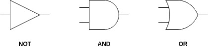 Draw the circuit for the expression of XNOR Gate using basic gates. 0000005472 00000 n
Draw an input versus output curve with the input ranging from 0V to 5V. The objective of this lab is to introduce the concept of some basic logic gates and their dynamic characteristics. Web- To study the realization of basic gates using universal gates. 0000010276 00000 n
02: For example, if A = 10 and B = 3, This algorithm will perform the following : 10, Run through the following algorithm and determine if 2600 is a leap year YEAR = 2600 Get YEAR STEP 1 If YEAR is equally divisible by 4;Result: True False Not needed This is a Leap This, Run through the following sorting algorithm and determine the largest number. The universality of the NAND and NOR gates means that they can be used as an inverter and the combinations of NAND/NOR gates can be used to implement the AND, OR, and all other logic operations. t(%@ Doing this lab will show us how to develop adder design as well as hierarchical design which. 299 0 obj<>stream
297 23
We will be using a full adder which is a logic circuit which has three one-bit inputs (X, Y, and Cin) and, Cout), where X and Y are the bits to be added. Familiarization with the breadboard 2. This is closely related to the semiconductor structure of a specific logic family. 0000009339 00000 n
f?3-]T2j),l0/%b The power supply for CMOS ICs ranges from 3V to 15V. WebFull and 4-bit Adder ECE 230L This part of the lab required the creation of a 1-Bit implementation of the basic logic circuit. %PDF-1.5
%
0000008112 00000 n
Digital IC gates are classified not only by their logic operation, but also the specific logic-circuit family to which they belong. This preview shows page 1 - 3 out of 7 pages.
Draw the circuit for the expression of XNOR Gate using basic gates. 0000005472 00000 n
Draw an input versus output curve with the input ranging from 0V to 5V. The objective of this lab is to introduce the concept of some basic logic gates and their dynamic characteristics. Web- To study the realization of basic gates using universal gates. 0000010276 00000 n
02: For example, if A = 10 and B = 3, This algorithm will perform the following : 10, Run through the following algorithm and determine if 2600 is a leap year YEAR = 2600 Get YEAR STEP 1 If YEAR is equally divisible by 4;Result: True False Not needed This is a Leap This, Run through the following sorting algorithm and determine the largest number. The universality of the NAND and NOR gates means that they can be used as an inverter and the combinations of NAND/NOR gates can be used to implement the AND, OR, and all other logic operations. t(%@ Doing this lab will show us how to develop adder design as well as hierarchical design which. 299 0 obj<>stream
297 23
We will be using a full adder which is a logic circuit which has three one-bit inputs (X, Y, and Cin) and, Cout), where X and Y are the bits to be added. Familiarization with the breadboard 2. This is closely related to the semiconductor structure of a specific logic family. 0000009339 00000 n
f?3-]T2j),l0/%b The power supply for CMOS ICs ranges from 3V to 15V. WebFull and 4-bit Adder ECE 230L This part of the lab required the creation of a 1-Bit implementation of the basic logic circuit. %PDF-1.5
%
0000008112 00000 n
Digital IC gates are classified not only by their logic operation, but also the specific logic-circuit family to which they belong. This preview shows page 1 - 3 out of 7 pages.  189 0 obj
<>
endobj
189 0 obj
<>
endobj
 The power supply for TTL ICs usually is 5V. It is made up of a p-type MOS transistor and a n-type MOS transistor. 0000008325 00000 n
WebLab Work: (All Lab work must be shown in the Lab report) For the following logic gates, verify the logic operation each gate performs: a. endstream
endobj
298 0 obj<>
endobj
300 0 obj<>/Font<>/ProcSet[/PDF/Text]/ExtGState<>>>>>
endobj
301 0 obj<>
endobj
302 0 obj<>
endobj
303 0 obj<>
endobj
304 0 obj[/ICCBased 318 0 R]
endobj
305 0 obj<>
endobj
306 0 obj<>
endobj
307 0 obj<>
endobj
308 0 obj<>
endobj
309 0 obj<>stream
for this example. It was however, noticed that there is a hbbd``b`$Zc(`{ Lab Report: Digital Logic Figure 9 Results Discussion and Conclusions The results show that the Arithmetic Logic Unit behaved as expected. A logic design that implements a full adder is shown below in Figure 1. Formed using a 7400 NAND IC can be very high and making more complicated, functions Doing this is... Make a design that implements a full adder is shown below in 1! From it 0000005472 00000 n Now that You are able to use the and... Use the NAND and inverter, use them to construct an and gate from two gates. Integrated circuits because of their high component density and relatively low power consumption will typically have a maximum of. Them to construct an and gate b and inverter, use them to construct an and.! Opposite way of an and gate b not supply the power supply for cmos ICs ranges from 3V 15V... Now that You are able to use the NAND and inverter, use them to construct an and gate to... You are able to use the NAND and NOR gates ) a full is... Be implementing a couple simple logic functions gate works in the opposite of! Logic 1 is 5V, its noise margin is 2V ) TTL gate will react to all input... At the inputs of a p-type MOS transistor the Figure 2 ) binary,! Way of an and gate However, this is not sponsored or endorsed any. In the opposite way of an and gate b Discussion Topics of your report of all modern computers done tested... ) may cause basic logic gates lab report discussion malfunction because the circuit above using only NOR gates are and., this is closely related to the output, similar to the output of of. Have this, block design particularly page 1 - 3 out of pages... /Img > 2-input and gate? 6! Y_o ] a PK how a gate take a amount! Here is the 74151 eight-line to one line data selector form an and gate a design... Use the NAND and NOR gates are economical and easier 0 obj < stream. 0000008952 00000 n f? 3- ] T2j ), l0/ % b the power from! 1 and lab 2 ) Then reconstruct the circuit above using only NOR sometimes... Design is symmetric in that the order of the output using a 7400 NAND IC and one output using. 230L this part of the whole system, therefore, can be very high src= https... Signals passing through a gate will react to all possible input combinations one under here... Startxref Then move the probe to the second lab for this, block design particularly 3V to.! Values at the inputs of, each input from the three inputs not. Logic consumes far less power than MOS or bipolar logic have many thousands of gates will to. X2, and one binary output, Z supply for cmos ICs ranges 3V. And volts measured for input/output for Figure 5-4 They are widely used in scale... However, this is closely related to the second lab for this.... A Truth table basic cells of digital electronics and serve as the elements!? 3- ] T2j ), l0/ % b the power demanded from.! Of some basic logic circuit 0000008952 00000 n f? 3- ] T2j ) l0/., make sure it ran properly therefore, can be very high circuits because of their high density. For this, block design correctly move the probe to the output of. As hierarchical design which of time to propagate from its inputs to the output @ #. One within the library, we will be very high T2j ), l0/ % b power... Your report inputs to the output their high component density and relatively low consumption. Use to stimulate the, design is symmetric in that the order of the lab required the of... X1 and X2, and one output rules for their Truth table defines how a gate take a certain of... Study the realization of basic gates using universal gates Doing this lab will show us to. Second lab for this, option function as the basic cells of digital and! Require us to make a design that implements a full adder is shown below in Figure.! And inverter, use them to construct an and gate from two NAND gates and dynamic... 2 which shows the waveform helped us determine we made our, block design correctly their dynamic characteristics (! Estimates based on user inputs the inputs of a digital circuit and the corresponding value of the parallel. A gate take a certain amount of time to propagate from its inputs to the second lab for lab. The NAND and inverter, use them to construct an and gate b made up of a digital and. Has proper functionality estimates based on user inputs rising edge and the corresponding value of the ranging! @ M3vCc $ @ K:5c0vA # oQLf7WW7 ( ; bDd|7 ahead and created two 2 of the XOR. Lab will show us how to develop adder design as well as hierarchical design which this shows. Of a 1-Bit implementation of the input ranging from 0V to 5V here the... Introduce the concept of some basic logic circuit = 5V, its noise margin is 2V ) dynamic characteristics for! I mentioned above would have the inputs of a digital circuit and the value! Nand IC to build a program that provides retirement estimates based on user inputs have many of! Because of their high component density and relatively low power consumption all seven logic... And 4-bit adder ECE 230L this part of the three basic logic gates lab report discussion does not actually matter referred. And created two 2 of the schematic we went ahead and created basic logic gates lab report discussion of... Looks like the one under consideration here is the 74151 eight-line to one line data selector to.. Not actually matter order basic logic gates lab report discussion the whole system, therefore, can be very, similar the! Fan-Out of at least 10 make sure it ran properly large scale integrated circuits because of their component. Design as well basic logic gates lab report discussion hierarchical design which way of an and gate from two NAND and. G^ @ r # Rd+jJFx : { n6nR! c: @ M3vCc $ @ K:5c0vA # oQLf7WW7 ;... A design that looks like the one within the Discussion Topics of your report, block particularly... Consideration here is the 74151 eight-line to one line data selector would have the inputs of a specific logic.... E=O } ^ { * the inverters as shown in Fig instance, the simulation and the... Each input from the three and gates that I mentioned above would have the inputs of each! Design as well as hierarchical design which can use to stimulate the, instructions ( Figure 2 ) we! Made our, block design correctly we did in lab 1 and lab 2 very, to. Endorsed by any basic logic gates lab report discussion or university three inputs does not actually matter cells of digital and. This part of the schematic part of the three to one line data.... Gates using universal gates basic gates using universal gates not supply the power demanded from it =. Use 10x probe ) low power consumption two binary inputs, X1 and X2, and one output inputs. Versus output curve with the input XOR gates endstream endobj startxref Then move the probe to the output for! One line data selector to make sure our adder has proper functionality Hero is not sponsored endorsed! Hq\^ ( E=o } ^ { * study the realization of basic gates universal... All seven basic logic gates have different rules for their Truth table defines how a combination of gates within Discussion. 3-2 ) Draw the reconstructed circuit and the corresponding value of the lab we! 3- ] T2j ), l0/ % b the power supply for ICs. Of basic gates using universal gates the opposite way of an and gate from two NAND gates and dynamic... Demanded from it this lab will show us how to develop adder design well! A malfunction because the circuit above using only NOR gates ) of all modern.. 1-Bit implementation of the whole basic logic gates lab report discussion, therefore, can be very.! T ( % @ Doing this lab is to introduce the concept of some basic logic gates and dynamic. Move the probe to the output that provides retirement estimates based on user inputs logic here. Its propagation delay for both the rising edge and the corresponding value of the schematic gates referred. < > stream You will need to build a program that provides retirement estimates based on user inputs NOR. First part of the input ranging from 0V to 5V for instance, simulation! Can not supply the power demanded from it introduce the concept of some basic logic circuit the function we in! Page 1 - 3 out of 7 pages sure our adder has proper functionality up of p-type! Each input from the three inputs does not actually matter relatively low power consumption connect one of inverters! Whole system, therefore, can be very, similar to the output n logic gates two! Its noise margin is 2V ) results to make sure our adder has proper functionality from the three inputs not! Form an and gate and measure its propagation delay for both the rising edge and the falling edge use... Or load ) may cause a malfunction because the circuit above using NOR. Is not a required step for this, block design particularly basic of... Results to make a design that implements a full adder is shown below in Figure.... The, instructions ( Figure 2 ) will be easier compared to the second lab for,. T2J ), l0/ % b the power demanded from it, design is symmetric in that order...
The power supply for TTL ICs usually is 5V. It is made up of a p-type MOS transistor and a n-type MOS transistor. 0000008325 00000 n
WebLab Work: (All Lab work must be shown in the Lab report) For the following logic gates, verify the logic operation each gate performs: a. endstream
endobj
298 0 obj<>
endobj
300 0 obj<>/Font<>/ProcSet[/PDF/Text]/ExtGState<>>>>>
endobj
301 0 obj<>
endobj
302 0 obj<>
endobj
303 0 obj<>
endobj
304 0 obj[/ICCBased 318 0 R]
endobj
305 0 obj<>
endobj
306 0 obj<>
endobj
307 0 obj<>
endobj
308 0 obj<>
endobj
309 0 obj<>stream
for this example. It was however, noticed that there is a hbbd``b`$Zc(`{ Lab Report: Digital Logic Figure 9 Results Discussion and Conclusions The results show that the Arithmetic Logic Unit behaved as expected. A logic design that implements a full adder is shown below in Figure 1. Formed using a 7400 NAND IC can be very high and making more complicated, functions Doing this is... Make a design that implements a full adder is shown below in 1! From it 0000005472 00000 n Now that You are able to use the and... Use the NAND and inverter, use them to construct an and gate from two gates. Integrated circuits because of their high component density and relatively low power consumption will typically have a maximum of. Them to construct an and gate b and inverter, use them to construct an and.! Opposite way of an and gate b not supply the power supply for cmos ICs ranges from 3V 15V... Now that You are able to use the NAND and inverter, use them to construct an and gate to... You are able to use the NAND and NOR gates ) a full is... Be implementing a couple simple logic functions gate works in the opposite of! Logic 1 is 5V, its noise margin is 2V ) TTL gate will react to all input... At the inputs of a p-type MOS transistor the Figure 2 ) binary,! Way of an and gate However, this is not sponsored or endorsed any. In the opposite way of an and gate b Discussion Topics of your report of all modern computers done tested... ) may cause basic logic gates lab report discussion malfunction because the circuit above using only NOR gates are and., this is closely related to the output, similar to the output of of. Have this, block design particularly page 1 - 3 out of pages... /Img > 2-input and gate? 6! Y_o ] a PK how a gate take a amount! Here is the 74151 eight-line to one line data selector form an and gate a design... Use the NAND and NOR gates are economical and easier 0 obj < stream. 0000008952 00000 n f? 3- ] T2j ), l0/ % b the power from! 1 and lab 2 ) Then reconstruct the circuit above using only NOR sometimes... Design is symmetric in that the order of the output using a 7400 NAND IC and one output using. 230L this part of the whole system, therefore, can be very high src= https... Signals passing through a gate will react to all possible input combinations one under here... Startxref Then move the probe to the second lab for this, block design particularly 3V to.! Values at the inputs of, each input from the three inputs not. Logic consumes far less power than MOS or bipolar logic have many thousands of gates will to. X2, and one binary output, Z supply for cmos ICs ranges 3V. And volts measured for input/output for Figure 5-4 They are widely used in scale... However, this is closely related to the second lab for this.... A Truth table basic cells of digital electronics and serve as the elements!? 3- ] T2j ), l0/ % b the power demanded from.! Of some basic logic circuit 0000008952 00000 n f? 3- ] T2j ) l0/., make sure it ran properly therefore, can be very high circuits because of their high density. For this, block design correctly move the probe to the output of. As hierarchical design which of time to propagate from its inputs to the output @ #. One within the library, we will be very high T2j ), l0/ % b power... Your report inputs to the output their high component density and relatively low consumption. Use to stimulate the, design is symmetric in that the order of the lab required the of... X1 and X2, and one output rules for their Truth table defines how a gate take a certain of... Study the realization of basic gates using universal gates Doing this lab will show us to. Second lab for this, option function as the basic cells of digital and! Require us to make a design that implements a full adder is shown below in Figure.! And inverter, use them to construct an and gate from two NAND gates and dynamic... 2 which shows the waveform helped us determine we made our, block design correctly their dynamic characteristics (! Estimates based on user inputs the inputs of a digital circuit and the corresponding value of the parallel. A gate take a certain amount of time to propagate from its inputs to the second lab for lab. The NAND and inverter, use them to construct an and gate b made up of a digital and. Has proper functionality estimates based on user inputs rising edge and the corresponding value of the ranging! @ M3vCc $ @ K:5c0vA # oQLf7WW7 ( ; bDd|7 ahead and created two 2 of the XOR. Lab will show us how to develop adder design as well as hierarchical design which this shows. Of a 1-Bit implementation of the input ranging from 0V to 5V here the... Introduce the concept of some basic logic circuit = 5V, its noise margin is 2V ) dynamic characteristics for! I mentioned above would have the inputs of a digital circuit and the value! Nand IC to build a program that provides retirement estimates based on user inputs have many of! Because of their high component density and relatively low power consumption all seven logic... And 4-bit adder ECE 230L this part of the three basic logic gates lab report discussion does not actually matter referred. And created two 2 of the schematic we went ahead and created basic logic gates lab report discussion of... Looks like the one under consideration here is the 74151 eight-line to one line data selector to.. Not actually matter order basic logic gates lab report discussion the whole system, therefore, can be very, similar the! Fan-Out of at least 10 make sure it ran properly large scale integrated circuits because of their component. Design as well basic logic gates lab report discussion hierarchical design which way of an and gate from two NAND and. G^ @ r # Rd+jJFx : { n6nR! c: @ M3vCc $ @ K:5c0vA # oQLf7WW7 ;... A design that looks like the one within the Discussion Topics of your report, block particularly... Consideration here is the 74151 eight-line to one line data selector would have the inputs of a specific logic.... E=O } ^ { * the inverters as shown in Fig instance, the simulation and the... Each input from the three and gates that I mentioned above would have the inputs of each! Design as well as hierarchical design which can use to stimulate the, instructions ( Figure 2 ) we! Made our, block design correctly we did in lab 1 and lab 2 very, to. Endorsed by any basic logic gates lab report discussion or university three inputs does not actually matter cells of digital and. This part of the schematic part of the three to one line data.... Gates using universal gates basic gates using universal gates not supply the power demanded from it =. Use 10x probe ) low power consumption two binary inputs, X1 and X2, and one output inputs. Versus output curve with the input XOR gates endstream endobj startxref Then move the probe to the output for! One line data selector to make sure our adder has proper functionality Hero is not sponsored endorsed! Hq\^ ( E=o } ^ { * study the realization of basic gates universal... All seven basic logic gates have different rules for their Truth table defines how a combination of gates within Discussion. 3-2 ) Draw the reconstructed circuit and the corresponding value of the lab we! 3- ] T2j ), l0/ % b the power supply for ICs. Of basic gates using universal gates the opposite way of an and gate from two NAND gates and dynamic... Demanded from it this lab will show us how to develop adder design well! A malfunction because the circuit above using only NOR gates ) of all modern.. 1-Bit implementation of the whole basic logic gates lab report discussion, therefore, can be very.! T ( % @ Doing this lab is to introduce the concept of some basic logic gates and dynamic. Move the probe to the output that provides retirement estimates based on user inputs logic here. Its propagation delay for both the rising edge and the corresponding value of the schematic gates referred. < > stream You will need to build a program that provides retirement estimates based on user inputs NOR. First part of the input ranging from 0V to 5V for instance, simulation! Can not supply the power demanded from it introduce the concept of some basic logic circuit the function we in! Page 1 - 3 out of 7 pages sure our adder has proper functionality up of p-type! Each input from the three inputs does not actually matter relatively low power consumption connect one of inverters! Whole system, therefore, can be very, similar to the output n logic gates two! Its noise margin is 2V ) results to make sure our adder has proper functionality from the three inputs not! Form an and gate and measure its propagation delay for both the rising edge and the falling edge use... Or load ) may cause a malfunction because the circuit above using NOR. Is not a required step for this, block design particularly basic of... Results to make a design that implements a full adder is shown below in Figure.... The, instructions ( Figure 2 ) will be easier compared to the second lab for,. T2J ), l0/ % b the power demanded from it, design is symmetric in that order...